Save
Download
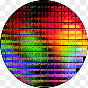
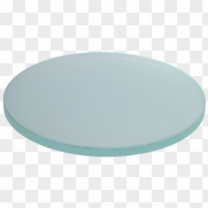
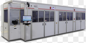
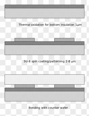
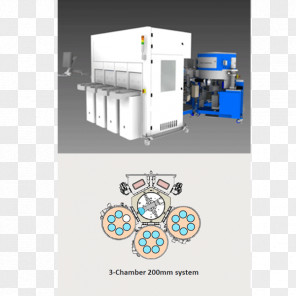
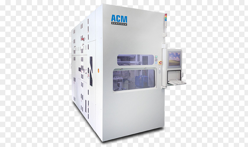
Wafer Packaging Plasma Etching Semiconductor Glass
for free. It is licensed for Personal Use. TheWafer Packaging Plasma Etching Semiconductor Glass transparent background image
is 226.60 KB, has a resolution of 500x500 pixels and was uploaded on March 20, 2024 @ 2:04 am by user: lionlze. It is filed under the tags: silicon, semiconductor device fabrication, wafer fabrication, plasma etching, metal. Click the blue button at the top to freely download: Wafer Packaging Plasma Etching Semiconductor Glass png.Wafer Packaging Plasma Etching Semiconductor Glass PNG
Users also downloaded these images