Save
Download
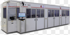
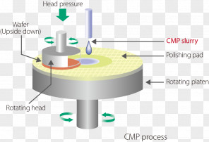
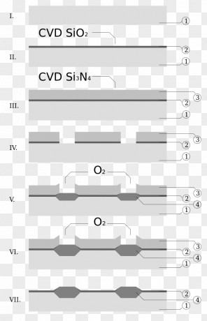
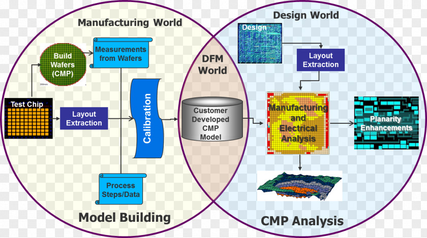
Technology Chemical-mechanical Planarization Front End Of Line Back Semiconductor High-κ Dielectric
for free. It is licensed for Personal Use. TheTechnology Chemical-mechanical Planarization Front End Of Line Back Semiconductor High-κ Dielectric transparent background image
is 441.26 KB, has a resolution of 1443x806 pixels and was uploaded on December 31, 2023 @ 7:46 pm by user: jonoig. It is filed under the tags: technology, 22 nanometer, semiconductor device fabrication, wafer, engineering. Click the blue button at the top to freely download: Technology Chemical-mechanical Planarization Front End Of Line Back Semiconductor High-κ Dielectric png.Technology Chemical-mechanical Planarization Front End Of Line Back Semiconductor High-κ Dielectric PNG
Users also downloaded these images