Save
Download
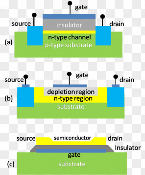
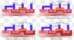
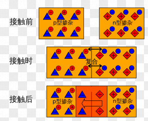
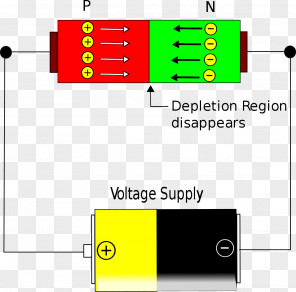
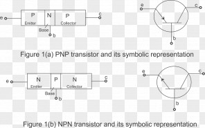
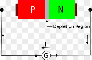
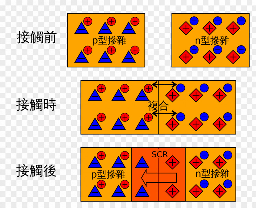
Junction P–n P-type Semiconductor Charge Carrier Depletion Region
for free. It is licensed for Personal Use. TheJunction P–n P-type Semiconductor Charge Carrier Depletion Region transparent background image
is 135.03 KB, has a resolution of 1255x1024 pixels and was uploaded on March 20, 2024 @ 3:15 pm by user: ernafher. It is filed under the tags: recreation, electric potential difference, area, electronic component, electronics. Click the blue button at the top to freely download: Junction P–n P-type Semiconductor Charge Carrier Depletion Region png.Junction P–n P-type Semiconductor Charge Carrier Depletion Region PNG
Users also downloaded these images